

Blog
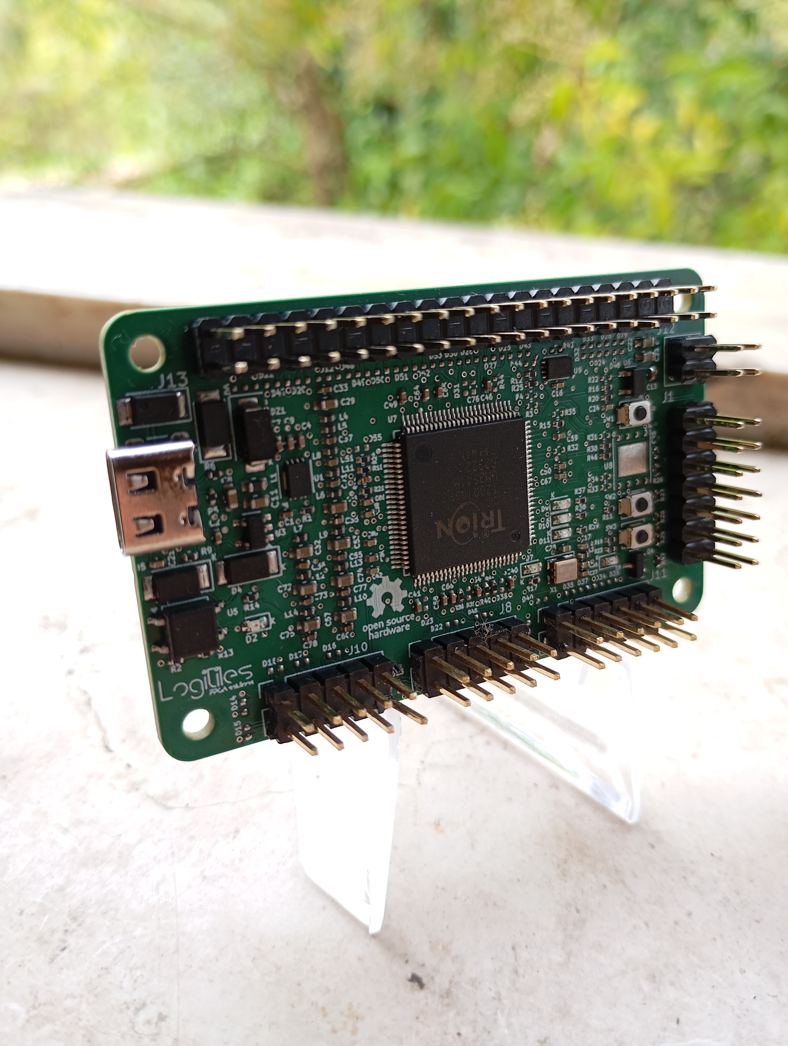
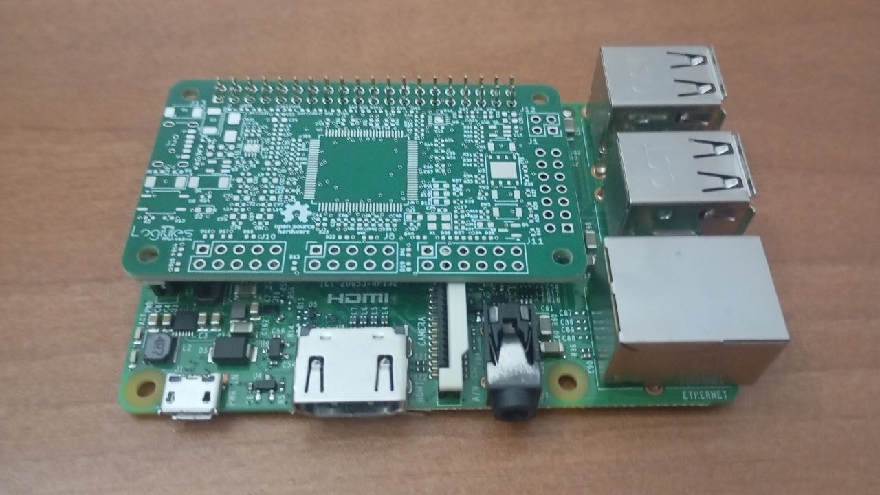
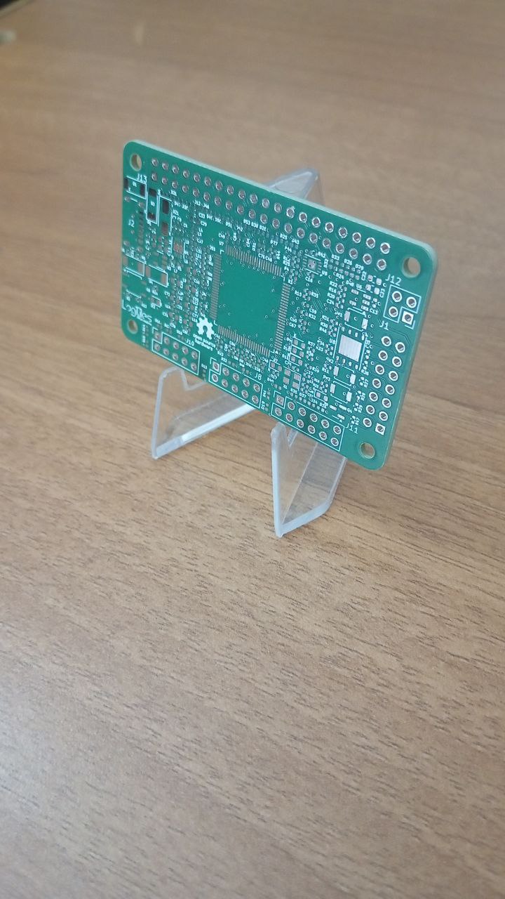
We are extremely proud to announce that we have just started building the first version of the HEXCHOOL-20Q100, a board dedicated to those who want to learn how to design with FPGAs, and that will be provided to students of our FPGAcademy included in the price of the courses.

This board was born in the wake of the success of our HEXBERRY-V board, which was presented at the Maker Faire 2024 held in Rome a few weeks ago. We wanted to provide students with a board that was slightly larger (it does not need to be as small as Hexberry-V) and with a greater presence of interaction peripherals for the students (buttons, leds,..). In addition, 2 PMOD interfaces (12 pins) and also 2 PMOD interfaces (6 pins) have been added, so that students will be able to learn how to design with FPGAs by interacting with any of the PMOD interfaces they want to use for their course/project.
Obviously this board can also be used as EVALUATION BOARD or as DEVELOPMENT BOARD, then delegating to HEXBERRY-V to represent the project in the product or creating a custom board for the purpose.

Like its sister board HEXBERRY-V, we expect that HEXCHOOL will be able to accommodate the 32-bit Efinix VexRisc processor, taking up roughly half of the available FPGA. This will allow our students to learn to design with a SoC as well, using tools like EFINITY and its Eclipse-based Efinity's RISC-V IDE plugin.
Note: these tools are and will always be free for HEXCHOOL, for HEXBERRY-V and for any FPGA coming from EFINIX
The main features of HEXCHOOL board are:
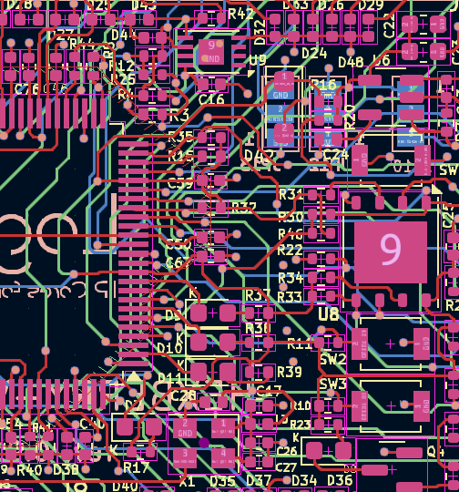
- dim. 80 x 70 mm
- EFINIX TRION T20Q100 Fpga
- 16Mb SPI flash INTERNAL to the FPGA
- external 50 Mhz oscillator
- 5V power supply via USB-C connector (for power only)
- 16 Mbit SPI flash memory (holds up to 2 full bitstreams) INTERNAL to the FPGA
- 4 buttons
- 4 LEDs
- 2 PMOD (12 pins) + 2 PMOD interfaces (6 pins)
- Low voltage supervisor with adjustable reset delay and manual reset
- Microchip cryptographic authentication IC
- USB-C to SPI (active and passive) and JTAG (bridge and direct) programmer on board (does not require an external programmer)
- Native I2C interface
NOTE: We are not affiliated with EFINIX inc. All product names, logos, and brands are property of their respective owners.
All companies, products and services names used in this website are for identification purposes only.
Welcome to Logitiles' FPGAcademy!
We provide courses that aim to teach the designers who will participate a design methodology with FPGA with an industrial approach (placing the student colleagues in front of classic design situations that they will find themselves in the company when they are asked to carry out the system design).
Our teaching material is intended for use with our HEXchool board, which will be delivered to students who have purchased participation in the course, included in the price of the course itself. The material will be provided free of charge to students exclusively in electronic format, including the exercise sources, waveforms and bitstreams ready for use.
We suggest you subscribe to our newsletter to be constantly updated on our news, and prepare to become a member of the LOGITILES FPGAcademy, purchasing your first in-person course on digital design with FPGA.
The first two courses that will be available at the beginning of 2026 will be:
- VERILOG Basic (cod. F2.1): An overview of the Verilog language (version 2005) will be provided through extensive use of design examples, highlighting common errors that inexperienced designers make at the outset and demonstrating the results these errors create in synthesis. The tools for successful design will be provided, using verification and validation tools, in preparation for the transition to the SYSTEM VERILOG language, de facto being new version of the Verilog language. EFINIX and AMD design tools will also be used.
In the next few weeks we will announce the course Prices and schedule for multiple participation. For each course we will announce the list of topics and the duration of each one.
We are preparing to build the new version (0.91) of the HEXBERRY-V board. The debugging phase that we have just finished had highlighted possible improvements that we wanted to introduce in this new release. The final version (1.0) that will go into production is getting closer and closer, and its announcement will not take long.
STAY WITH US as usual...
We have completed the prototyping phase of the new release to present it at the Maker fair in Rome on October 24th. In this version we have replaced the 8 KLE FPGA with a much larger 20 KLE one. This then has the ability to include FLASH memory inside it where the designer can keep his bitstream without the fear that someone can easily take possession of it with sniffing activities, or that it can be corrupted by malicious people with penetration attacks. In addition, we have switched to the use of a USB-C connector with which to supply power to the board. In this release we have also activated the dual programming mode of the FPGA with both JTAG and SPI communication, in order to provide more flexibility to the designer, especially in case he needs to insert the VEXRISC-V processor into the FPGA.
Many edge-based applications necessitate low latency, alongside the ability to process substantial amounts of data from devices.
With 20+ years of experience in FPGA domain, Logitiles tables a strong & unparalleled FPGA Design-to-Deployment competence, possessing extensive proficiency in utilizing FPGA devices.
As a turnkey product design firm, we offer FPGA Designs tailored to meet clients specification which includes RTL Design, Integration of Logitiles’s or 3rd Party IP Cores on our FPGA SOMs with Carrier Card / Custom Hardware / Off-the-Shelf Evaluation Kits to provide end-to-end solutions targeting Low-Power, High-Performance and Optimized Designs.

Our expertise lies specifically in Aerospace and defense applications, specializing in developing FPGA accelerators for machine learning and communications algorithms. These accelerators empower the creation of real-time, low-latency, and power-efficient systems. In addition, our expertise in software design enables us to create SoC (System on Chip) solutions when needed.
Furthermore, we can establish a design flow and deliver designs in accordance with relevant industry standards:
- understanding the design intent and document it for client approval
- coding the design using proven coding styles
- Creating a custom testbench and verify all functionality of the design
- Reviewing coverage metrics and code coverage to achieve 100% effective coverage
- Reviewing IO driver selection with Foresys Signal Integrity Expert

Logitiles offers a wide range of FPGA design services from full turn-key development to individual services including:
- Architecture development
- RTL coding in Verilog, System Verilog or VHDL
- Embedded processor integration
- Verification in VHDL or System Verilog OVM, UVM, or VMM
- Synthesis
- Floorplanning
- Place and Route
- Lab Diagnostics
When you engage with Logitiles on a logic design, you should expect a short integration period. We are able to avoid a protracted diagnostic period by communicating the design accurately to other members of your design team. This is especially true when a design involves a complex software interface. We provide your development team with software routines to interface to the FPGA which help eliminate incompatibilities that teams often experience during integration.
We do our job right the first time. We stand behind our turnkey FPGA designs with a no-excuses warranty. Our clients do not pay us to fix mistakes; they pay us to do it right the first time. We do this by assigning only highly trained principal engineers who have the skills to complete the job quickly and accurately.
Receive a detailed fixed-price quote for FPGA development services
![]()
We are a team of senior engineers with more than forty years of combined experience in some of the most demanding and innovation‑driven industries, including Aerospace, Medical Technologies, Telecommunications and Industrial Automation. Working in these high‑reliability sectors has shaped our engineering culture: precision, robustness and long‑term performance are the foundation of everything we build.
A core part of our expertise lies in FPGA design, verification and system integration. Over the years, we have developed custom IP cores, high‑performance digital architectures and embedded processing pipelines for clients who require deterministic behavior, low latency and absolute reliability. Our experience spans the full FPGA lifecycle: RTL design in VHDL/Verilog/System Verilog, advanced verification (UVM,Cocotb,OSVVM,UVVM), timing closure, resource optimization and integration into complex SoC and edge‑AI platforms.
We have delivered FPGA‑based solutions for applications such as high‑speed data acquisition, real‑time signal processing, sensor fusion, industrial control, secure communication and hardware acceleration. Our team works confidently across major FPGA families — Xilinx, Intel, Lattice, Microchip, Efinix — and with both proprietary and open‑source toolchains.
Beyond FPGA development, we bring a multidisciplinary approach to every project. We design complete electronic systems, from concept to prototype, combining hardware, firmware, embedded software and system‑level validation. This allows us to deliver solutions that are not only technically advanced, but also practical, integrable and ready for real‑world deployment.
Our work is guided by a set of values that define who we are and how we operate:
-
Transparency, because clear communication and full visibility are essential for building trust.
-
Professionalism, reflected in our rigorous methodology, disciplined execution and commitment to excellence.
-
Honesty, which means giving clients realistic expectations, reliable assessments and solutions that truly fit their needs.
Above all, we stand on the client’s side. We approach every project as a partnership, not a transaction. We listen, we understand the operational context, and we work to anticipate risks and remove complexity. Our clients rely on us not only for our technical capabilities, but also for our integrity, our clarity and our dedication to delivering solutions that stand the test of time.
![]() PierFrancesco Santi (CTO)
PierFrancesco Santi (CTO)

PierFrancesco has successfully delivered high complex electronics and products for Defence Electronics, Medical, Space and IC Industries. He has extensive knowledge & experience in embedded systems & hardware design from concept to manufacture. Pier has a professional experience of over 25 years working in very demanding electronic industries like avionics, military, communications among others. His focus is on Edge AI and Cybersecurity worlds, high speed PCB layout, vision, embedded design around FPGA and VLSI implementations. Pier holds a Master's of Science in Electronic Engineering from "La Sapienza" University (Rome, Italy).